Introduction
A Logic gate is an electronic circuit designed by using electronic components like diodes, transistors, resistors, and more. As the name implies, a logic gate is designed to perform logical operations in digital systems like computers, communication systems, etc. A logic gate can take two or more inputs but produce only one output. The output of a logic gate depends on the combination of inputs and the logical operation that the logic gate performs. Following are the primary logic gates and their functions:
1. AND gate: It is one of the three basic logic gates. It performs the logical multiplication of the inputs applied to it. For two-input AND gate, the Boolean expression is given by,
Y=A.B
Where, A and B are inputs to the AND gate, while Y denotes the output of the AND gate.
We can generalize the expression to any number of inputs:
Y=A.B.C.D . . ..
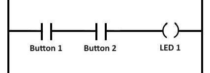
The truth table, symbol and ladder logic of a two input AND gate is shown below,
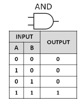
Truth Table 1
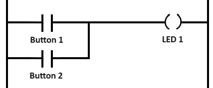
2. OR gate: OR gate is also one of the basic logic gates and its primary function is to perform logical addition. For a two input OR gate, the Boolean expression is given by,
Y=A+B
Where, A and B are inputs to the OR gate, while Y denotes the output of the OR gate.
We can generalize the expression to any number of inputs:
Y=A+B+C+D . . ..,
The truth table, symbol and ladder logic of a two input OR gate is shown below,
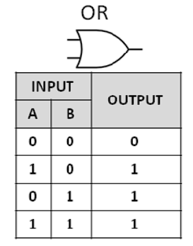
Truth Table 2
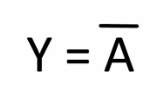
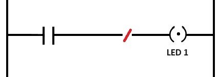
3. NOT gate: The NOT gate is another basic logic gate which performs complement of the input applied to it. It can take only 1 input unlike other logic. The output of the NOT gate is complement of the input applied to it. The NOT gate is also called an inverter, as it performs inversion operation. For a NOT gate, the Boolean expression is given by,
The truth table symbol and ladder logic of a two input OR gate is shown below,
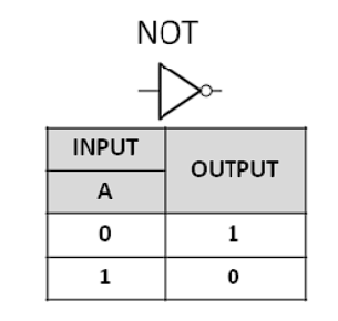
Table 3
4. NAND gate: It is another type of universal logic gate used to perform inverse AND operation. Similar to NOR gate, NAND gate can also have multiple inputs but only single output. NAND gate is an AND gate followed by a NOT gate. The Boolean expression of a two input NAND gate is as below:
The truth table, symbol and ladder logic of a two input OR gate is shown below,
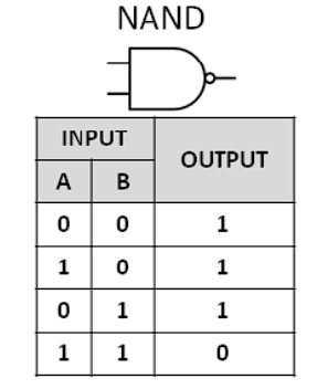
Truth Table 4
5. NOR gate: Its is one of the two universal gates. A universal gate is a logic gate whose combination can be used to make any other logic gate. A NOR gate is an OR gate followed by a NOT gate. A NOR gate can have multiple inputs and gives a single output. It gives a high or logic 1 output only when all of its inputs are low or logic 0. The Boolean expression of a two input NOR gate is as below:
The truth table, symbol and ladder logic of a two input OR gate is shown below,
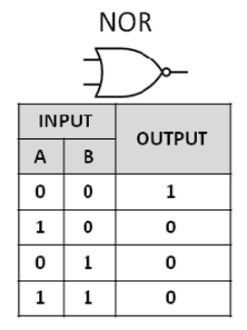
Truth Table 5
From this experiment onwards all the experiments will be simulated using a Programmable Logic Controller (PLC) as making control circuit of these experiments on an industrial panel (as done for the previous experiments) will be very complex.
A PLC is an industrial computing device used for managing electromechanical processes. A typical PLC consists of a power supply, CPU, Input/Output modules, ROM, RAM, and a programming device such as a PC. The input modules send an input signal into the PLC where it is processed by the CPU. The format of output data is specified by an application program implemented on the programming device.
Various programming languages are used to program the PLC. One such language is Ladder logic programming. It uses graphical diagrams, which look like an electrical schematic, are based on relay circuit hardware to express the logical structure of processes in PLC software applications.
A PLC monitors real-time data and is used in product assembly, packaging, motion control, batch control, machine diagnostics and testing, and robotics processes.
Circuit operation
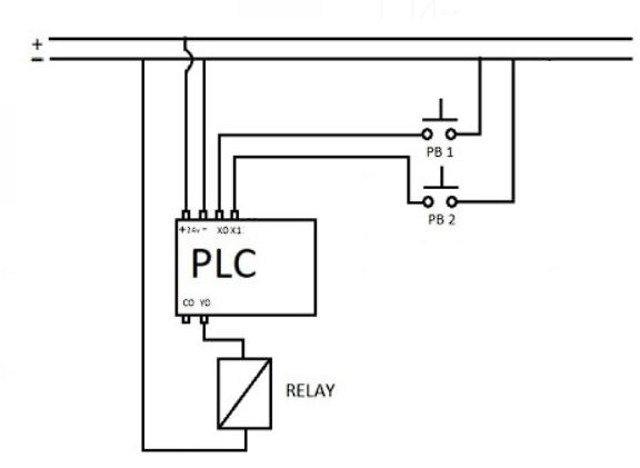
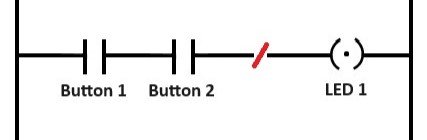
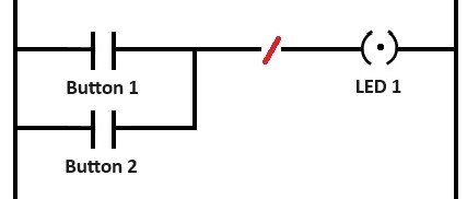
Fig. 6 The above control circuit will be used for the implementation of AND, OR, NAND, NOR logic gates only
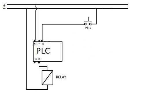
Fig. 7 The above control circuit will be used for the implementation of NOT logic gate only
Control circuit: The control circuit consists of a PLC module, a relay, two push-to-ON switches and a DC supply. The push-to-ON switches are connected between the positive of DC supply and input of the PLC (X0 and X1). The relay coil is connected to the output (Y0) of the PLC. The push-to-ON switches act as input device to the PLC. When the push button is pressed the input of PLC gets connected to the positive of the DC supply. This is taken as logic 1 or High in the Ladder logic program and the output is given to the relay according to the Ladder logic designed and implemented to the PLC.
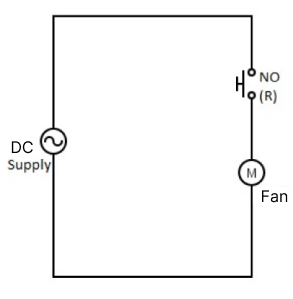
Power circuit: The power circuit consists of NO contact of relay in series with the DC load. When the output of the logic gate is logic 1 or High (according to its truth table) then output Y0 of the PLC will give a positive voltage and the relay will get energized. Once the relay energizes its NO contact will become NC and the DC load will turn ON. The DC load can be a Fan, Buzzer, etc.